When DDR5 memory entered the market, it brought both speed and complexity.
Compared to DDR4, DDR5 runs at much higher data rates.
The timing windows are tighter, and the voltage margins are smaller.
This means even small layout mistakes can have big consequences.
For layout engineers, this is where the difficulty begins.
The methods that worked fine for DDR4 no longer guarantee success.
A design that looks correct in CAD may fail in the lab with random errors, unstable operation, or sometimes a complete failure to boot.
The reason is simple.
At DDR5 speeds, the PCB itself becomes part of the circuit.
Every trace, via, and plane affects how signals behave.
If the layout is not carefully managed, signal integrity (SI) issues appear.
Let’s go through the most common DDR5 Signal integrity mistakes made during PCB layout.
Notice how one mistake often leads into the next, forming a chain of problems that reduce performance.
Common DDR5 SI Mistakes in Layout

Mistake 1: Poor Trace Impedance Control
The first mistake comes from ignoring impedance control.
DDR5 signals are designed for a specific impedance.
If the trace does not match this value, part of the signal reflects back.
These reflections distort the waveform, add jitter, and reduce timing margin.
In DDR4 designs, small mismatches were sometimes tolerated.
But with DDR5, the margins are so small that even slight deviations cause trouble.
Impedance depends on stackup, trace width, and spacing. If these are not planned and controlled carefully, the entire memory bus suffers.
Once impedance is not consistent, some signals arrive slightly later than others.
That directly creates the next issue—skew.
Mistake 2: Skew and Length Mismatch in Data Lines
DDR5 requires that data signals arrive in sync.
If one line is longer than the others, its signal is delayed.
This mismatch, called skew, reduces the available timing window for data capture.
At DDR5 speeds, even a few millimeters of extra length add enough delay to cause problems.
To fix skew, designers often stretch or shorten traces.
But here lies the risk—if you focus only on length matching and forget impedance, you solve one issue while creating another.
And when traces are adjusted in tight spaces, they are often pushed closer together.
That brings us directly to the next mistake: crosstalk.
Mistake 3: Crosstalk Due to Poor Spacing
At DDR5 frequencies, traces running close together easily interfere.
This interference, called crosstalk, makes signals noisy and unpredictable.
A victim trace can show false spikes or jitter simply because a neighbor switched rapidly.
Crosstalk becomes worse when length-matching forces traces into tight bundles.
If return paths are broken or not carefully planned, the effect grows stronger.
This shows how sensitive DDR5 is to noise.
But interference does not always come from neighboring traces.
Sometimes, the noise enters through the power itself—the PDN.
Mistake 4: Power Distribution Noise Coupling into DDR Nets
The power distribution network (PDN) is often treated as separate from signals, but in DDR5 designs, it is directly connected.
If the PDN is noisy, that noise couples into DDR signals.
The effect is jitter, false transitions, and unstable operation.
Many engineers think adding a few decoupling capacitors will solve this.
But with DDR5, it takes more—careful capacitor placement, low-inductance paths, and controlled return currents are all necessary.
If the PDN is noisy, even well-routed traces cannot perform correctly.
And when those traces use vias, a weak PDN combined with poor via design makes the problem worse.
Mistake 5: Inadequate Via Design (Stubs, Transitions, Non-Optimized Return Paths)
At high frequencies, vias are no longer simple connectors.
A poorly designed via introduces discontinuity.
If it leaves a stub—an unused via section—it reflects part of the signal back.
Vias can also disrupt return paths, forcing currents to take long detours, which adds both noise and delay.
This mistake does not stand alone.
Reflections from stubs make impedance mismatches worse.
Broken return paths increase crosstalk between nearby signals.
And PDN noise becomes harder to control when currents do not flow directly.
When vias are not optimized, the effectiveness of termination also suffers.
Mistake 6: Incorrect Termination Placement or Values
Termination is used to absorb reflections and stabilize signals.
But in DDR5, both the value of the termination resistor and its placement are critical.
If the resistor value does not match the trace impedance, or if it is placed incorrectly, reflections remain.
Once this happens, all the previous mistakes—improper impedance, skew, crosstalk, PDN noise, and via stubs—combine to overwhelm the signal.
The timing margin collapses, and the system becomes unreliable.
Impact of These Mistakes
When these layout mistakes add up, the result is costly.
Prototypes fail during testing. Timing closure is not achieved. The board may sometimes boot and sometimes fail.
Random errors appear in ways that are difficult to trace.
Fixing these problems after layout is expensive and slow.
Each re-spin costs time and money. Debugging is frustrating because solving one issue often exposes another.
The design cycle stretches longer, and confidence in the product decreases.
How to Avoid DDR5 Signal Integrity Mistakes

- Start With a Thoughtful Stack-UpDefine the stack-up before routing begins. DDR5 signal integrity requires controlled impedance (typically 50 Ω single-ended and 100 Ω differential).
Calculate trace widths and spacing based on dielectric thickness and copper weight.
Include dedicated ground planes adjacent to high-speed layers for stable return paths.
Lock the stack-up with your fabricator early to avoid last-minute impedance deviations.
- Ensure Uniform Trace LengthsSet tight length-matching constraints for DQ and DQS lines (typically within ±2–3 mils).
Use serpentine tuning with smooth bends (no sharp jogs) to compensate for length mismatches.
Always verify both propagation delay and intra-byte skew in simulation, not just raw length.
- Keep Signals Well-SpacedMaintain at least 3W spacing (three times the trace width) between high-speed DDR5 nets to minimize crosstalk.
Avoid long, parallel runs on the same layer. If parallelism is unavoidable, use orthogonal routing on adjacent layers.
Ensure uninterrupted ground reference under all high-speed routes to prevent return path discontinuities.
- Build a Strong Power NetworkDDR5’s narrow jitter margin demands a low-impedance PDN (<500 mΩ across the DDR frequency range).
Use target impedance profiles and verify with PDN simulation.
Place decoupling capacitors (0402 or 0201) close to VDD/VDDQ pins, connected with short, wide traces or via-in-pad.
Deploy a broad-band capacitor mix (bulk, mid-frequency, high-frequency) to suppress noise across the spectrum.
- Optimize Vias for Smooth TransitionsAvoid via stubs by using back-drilling or blind/buried vias. Keep signal vias short (<20 mils effective length for DDR5 frequencies).
Always provide a nearby return via next to each signal via to maintain continuous return paths.
Model via impedance in SI tools to identify discontinuities before fabrication. - Apply Proper Termination
Use ODT (On-Die Termination) wherever supported by DDR5 controllers, as it minimizes stub effects and reduces external resistor count.
When external resistors are required, place them within 200 mils of the driver/receiver. Match termination resistance to trace impedance (typically 50 Ω).
Validate resistor value and placement with SI simulation to confirm reflection damping. - Simulate Continuously
Integrate SI analysis into every design phase:
- Pre-layout → stack-up impedance planning, PDN impedance targets.
- During layout → check skew, crosstalk, reflections in critical byte lanes.
- Post-layout → eye diagram and timing margin analysis to confirm JEDEC compliance.
Leverage tools like S-parameter extraction for vias and IBIS/IBIS-AMI models for DDR5 controllers/DRAM.
Conclusion
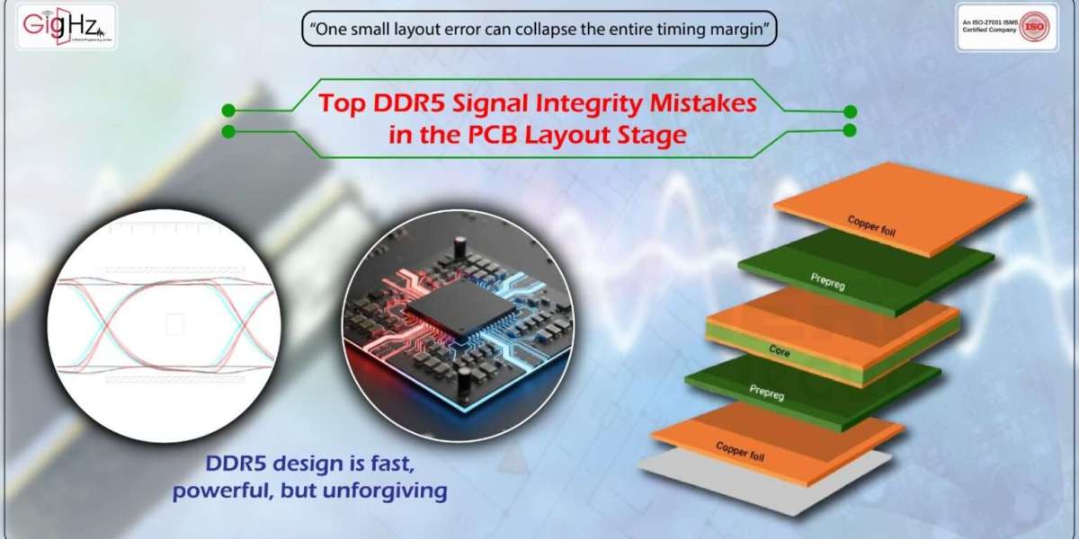
DDR5 design is fast, powerful, but unforgiving.
The mistakes we discussed—poor impedance control, skew, crosstalk, PDN noise, inadequate vias, and incorrect termination—are all connected.
One mistake often leads to another, shrinking the small margins DDR5 allows.
The only way to succeed is careful planning: follow design rules, optimize your stack-up, match trace lengths, control PDN noise, and verify signals through simulations.
By respecting signal integrity from the start, you ensure that DDR5 performs reliably, with speed, stability, and predictable operation.
Even a layout that looks perfect can fail if these principles are ignored, so early planning and disciplined design are essential for success.
This content is originally posted on: https://gighz.net/
Source URL: https://gighz.net/analysis-simulation/top-ddr5-signal-integrity-mistakes-in-the-pcb-layout-stage/