
When a PCB works in the lab but fails in the field, one of the common reasons is signal integrity.
Signals that look fine at first can become distorted, delayed, or noisy once the board is in real use.
These problems are not always obvious, but they directly affect reliability.
A board with poor signal integrity may still power on, but data errors, jitter, or random resets soon appear.
These issues are frustrating because they don’t always appear right away, yet they can make a product unreliable.
This is why signal integrity in the PCB design is not something to think about only at the end of design.
It has to guide your decisions from the very start.
In this guide, you will go step by step through the main areas of signal integrity.
Each part builds on the one before it, so by the end, you will have a clear path for designing reliable PCBs.
Step 1: Understand Signal Behavior at High Speed
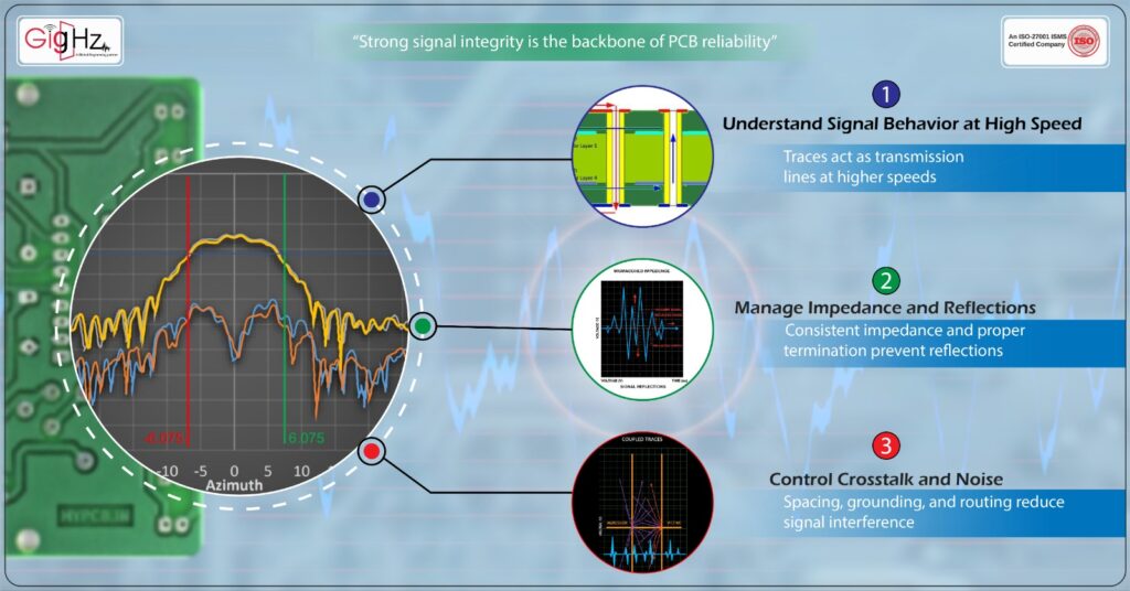
At low speeds, a PCB trace behaves like a simple wire, and signals travel without distortion.
But as data rates increase or rise times become faster, the same trace starts behaving as a transmission line, where the signal is influenced by the trace geometry, the PCB’s dielectric material, and the return path through the ground or power plane.
When the trace length becomes comparable to the signal rise time, effects such as reflections, ringing, and timing delays appear.
These issues are subtle but can cause significant data errors if ignored.
Recognizing this early ensures that subsequent design choices, such as trace layout and termination, are made with signal integrity in mind.
Once it is clear that a signal behaves as a transmission line, controlling impedance and managing reflections becomes critical.
This is the natural next step to ensure signals travel cleanly from driver to receiver.
Step 2: Manage Impedance and Reflections
Once you treat a trace as a transmission line, impedance becomes important.
A signal expects to see the same impedance from driver to receiver.
If the impedance changes, part of the signal reflects back. These reflections mix with the original signal and distort it.
To prevent this, you need two things.
The first is controlled impedance — define the PCB stackup early, set trace widths and spacing based on dielectric thickness, and check those values with the PCB fabricator.
The second is termination — depending on the standard, this may mean series resistors, parallel resistors, or on-die termination.
When impedance is consistent and reflections are absorbed, the signal moves forward cleanly.
But signals do not travel in isolation. On a PCB, they share space with many others, and that brings in the challenge of crosstalk.
Step 3: Control Cross-talk and Noise
Crosstalk happens when two signals are close enough that energy couples between them. One trace acts as the aggressor, the other as the victim.
The result is unwanted interference that reduces timing margin and clarity.
This effect is most common when traces run parallel for long distances.
You can reduce it by spacing high-speed traces apart, routing differential pairs closely to each other, and using ground planes to contain fields.
Routing signals on adjacent layers at right angles also reduces coupling.
Noise is not limited to trace interactions. It can also come from the power delivery network.
If the supply is unstable, that noise will appear in every signal.
This shows that signal integrity and power integrity are linked, which leads directly to the next step.
Step 4: Power Integrity and Decoupling
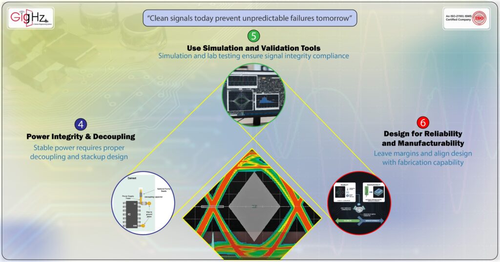
For signals to stay clean, the power network must stay stable.
Every signal uses the power and ground planes as its reference. If this reference is noisy, the signal itself loses clarity.
Decoupling capacitors are your main tool here. Large capacitors handle low-frequency shifts, while small capacitors filter high-frequency noise.
Placement matters as much as value — you need to place them close to the IC pins they support to minimize inductance.
The PCB stackup also supports power integrity. A power plane placed close to a ground plane creates natural capacitance, which lowers impedance and smooths the supply.
Once you create a stable power foundation, your signals have the support they need.
But design choices cannot stop at assumptions. Testing and validation are essential, which takes you to the next step.
Step 5: Use Simulation and Validation Tools
High-speed effects are not always visible until the board is running.
A trace that looks fine in layout may still introduce jitter, skew, or overshoot once fabricated.
That is why simulation and validation are essential.
Pre-layout simulation lets you test impedance and termination strategies before routing.
Post-layout simulation checks whether your routing choices and timing goals are actually met.
After fabrication, lab measurements — oscilloscopes, TDRs, and eye-diagrams — confirm the true behavior of your signals.
This may feel like extra effort, but it prevents redesigns and helps you catch problems before they reach production.
More importantly, it gives confidence that the design will behave as expected.
This confidence matters most when you move to the final step: designing for reliability and manufacturability.
Step 6: Design for Reliability and Manufacturability
Even if a design looks perfect in simulation and in the lab, it still needs to survive real-world conditions.
Reliability means leaving margin. Your signals should remain stable even when temperature changes, supply voltage shifts, or process variations occur.
Manufacturability is the other piece. Controlled impedance routing and stackups must match what the PCB fabricator can build consistently.
If there is a mismatch, signal integrity in the PCB design suffers across production.
Talking to your fabricator early ensures your design rules match fabrication capability.
By addressing both reliability and manufacturability, the design moves from something that works on paper into something that performs consistently in practice.
Bottom Line
Signal integrity is not a final check at the end of design. It is a continuous thread that runs through every stage of PCB development.
It starts with understanding how signals behave as transmission lines. That leads naturally into impedance control and reflection management.
Once that is addressed, you must deal with crosstalk, since signals always share space with others.
Power integrity follows, because every signal depends on a stable reference.
Simulation and validation then prove that your design decisions actually hold up.
Finally, reliability and manufacturability ensure your signals remain stable not just once, but across real conditions and production batches.
A PCB with good signal integrity is one that behaves predictably.
And predictability is what creates reliability.
This content is originally posted on: https://gighz.net/
Source URL: https://gighz.net/analysis-simulation/signal-integrity-in-the-pcb-design-a-guide-for-reliable-pcbs/