
Nowadays, most engineers assume that if their schematic checks out and the layout looks clean, then they are completely safe.
However, there’s a major catch here that some of the most expensive PCB design mistakes don’t show up until they are deep into prototyping or production.
Now, you may have probably followed the ECAD design process exactly as the datasheets and guidelines suggested.
But your board still ends up underperforming, or worse!
Failing completely in real-world use cases. So what really went wrong you think?
It’s Not the Circuit! It’s What Happens After the Circuit
Well, most design teams focus almost entirely on functionality but “Does the circuit work on paper as well?” or “Does the signal flow even logically?”
Whereas, the truth is that many boards fail not because of the design logic but because of physical factors like:
- Return paths
- Trace geometries,
- EMI coupling
- Mechanical alignment.
Moreover, these issues often go undetected until the cost of fixing them is at its peak.
Evidently, a shocking number of issues stem from ignoring signal integrity in PCB design. In fact, many of the failures we’ve seen looked perfect in simulation but couldn’t survive even basic field testing.
The Frustration: “But Everything Passed DRC!”
Now, let me share a real scenario that we went through.
So, we worked with a startup building a power-dense embedded system. Likewise, the engineer followed the ECAD design process meticulously. Plus, the schematic was flawless and the layout was tidy. In addition, the Gerbers looked clean and the DRC showed zero errors.
But want to know what happened during bring-up? Well, It started with:
- Random system resets
- Noise in analog readings
- Failures above 45°C ambient
After the investigation, we found it wasn’t a logic problem! Instead it was a combination of signal integrity in PCB design issues and overlooked PCB prototyping errors:
– High-speed lines routed near board edges
– Poor via stitching across return paths
– Solder mask alignment issues causing shorts
Now, by the time the root cause was identified, they had already ordered 3 prototype batches and lost 6 weeks.
The Fix
So, here’s a way to spot (and prevent) such critical bottlenecks:
1. Prioritize Return Paths Early
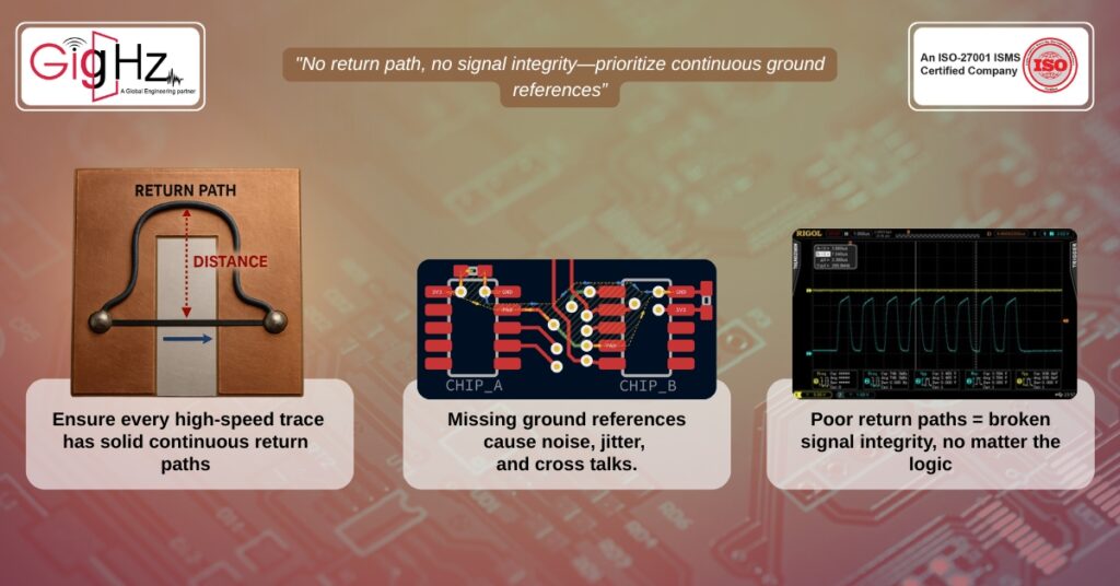
So, if you’re routing high-speed signals, make sure that every trace has a solid, continuous return path.
As, the absence of a nearby ground reference is a primary cause of noise, jitter, and crosstalk.
Most importantly, this is non-negotiable in signal integrity in PCB design.
2. Don’t Skip Stack-Up Planning
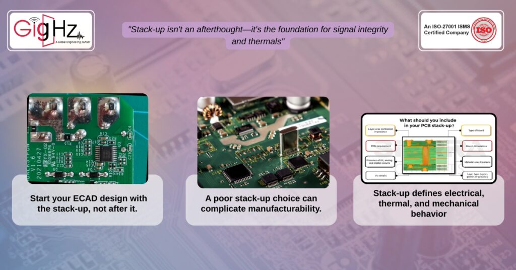
Now, layer arrangement affects more than just impedance!
Eventually, it affects thermals, EMI, and manufacturability as well.
So, the ECAD design process should begin with stack-up definition, not end with it.
3. Simulate with the Right Models
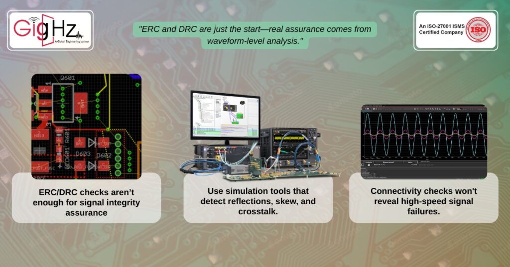
Besides, basic ERC and DRC checks won’t catch what real signal integrity in PCB design simulations can.
Hence, always consider using SI tools like HyperLynx ir Ansys SI wave that captures reflections, skews, crosstalks, and not just connectivity.
4. Validate Against Real-World Stress
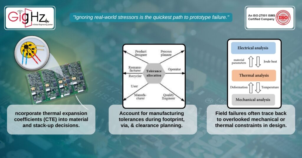
Now, what passes in a lab might fail eventually in the field at times. So, consider accounting for mechanical stress, vibration, thermal expansion, and manufacturing tolerances. As many PCB prototyping errors are due to ignoring these during design.
Bottom Line
Summing up, so what’s dangerous about PCB prototyping errors is how quietly they sneak in. Evidently, a board may power up and pass the basic tests, only to fail weeks later in the field.
And the worst part? By then, you’re already dealing with lost time, lost trust, and budget blowouts. Also, a perfect schematic can’t protect you from physical-layer problems that disrupt your product’s performance.
Therefore, you must consider having a second set of eyes on your next design! Likewise, our DFM and SI-focused layout review catches the PCB design mistakes that most tools miss.
This content is originally posted on: https://gighz.net/
Source URL: https://gighz.net/ecad/the-secret-reason-most-pcb-designs-fail-isnt-what-you-think/