Introduction: The Silent Backbone of Modern Electronics
From Circuitry to Innovation Catalyst
Hidden beneath the sleek veneer of every smartphone, tablet, data server, or electric vehicle lies a marvel too often overlooked—advanced semiconductor packaging. It’s the uncelebrated hero that breathes connectivity into our daily lives, quietly engineering the power, performance, and miniaturization we now take for granted.
for more inform : https://market.us/report/global-advanced-packaging-market/
Why Advanced Packaging Matters More Than Ever
As Moore’s Law slows, and demand for performance-intensive applications accelerates, traditional chip scaling alone cannot keep up. Enter advanced packaging—a transformative shift from mere protection to performance orchestration. It enables chips to be smaller, faster, cooler, and smarter. Not a luxury, but a necessity in tomorrow’s tech race.
Defining Advanced Packaging: Beyond the Traditional Mold
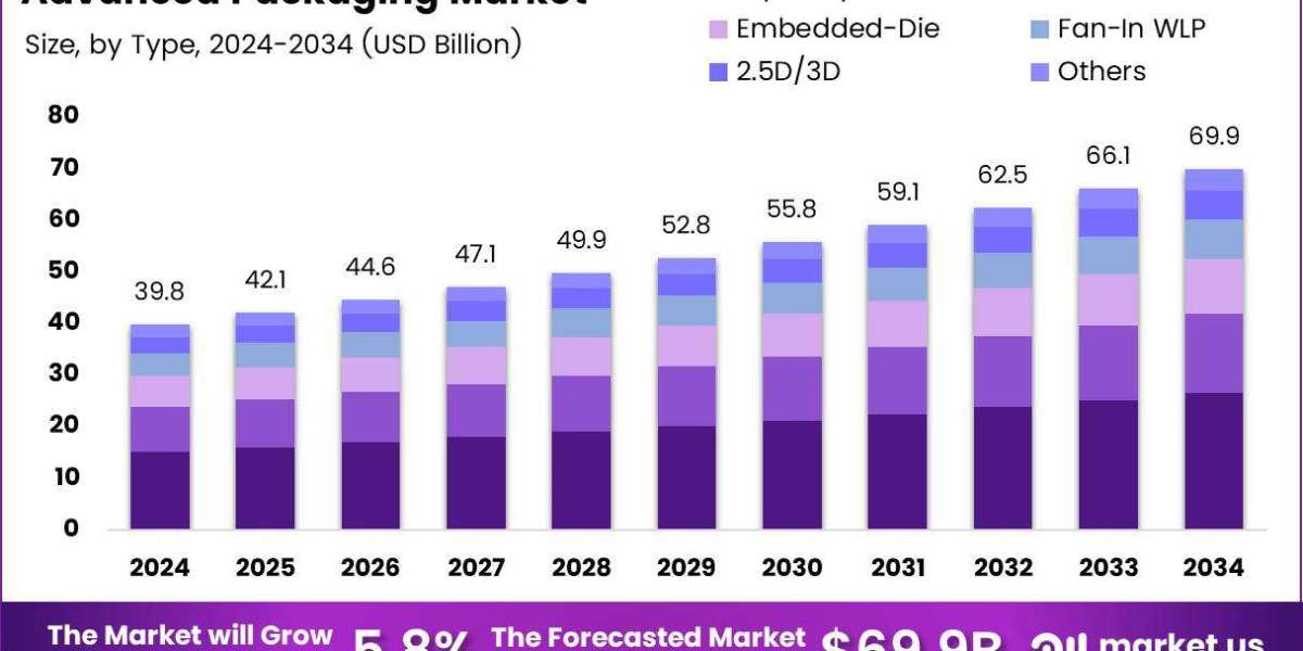
Key Technologies: 2.5D, 3D, Fan-Out, and System-in-Package
Advanced packaging isn't a monolith—it’s a mosaic of techniques. 2.5D uses interposers to connect multiple chips side-by-side. 3D stacking goes vertical, shrinking footprints and shortening interconnect distances. Fan-Out Wafer-Level Packaging (FOWLP) enhances power efficiency and reduces form factors. And System-in-Package (SiP) consolidates diverse components into a compact ecosystem-on-a-chip.
Each format answers a specific performance equation—and together, they are rewriting what chips can do.
The Shift from Interconnects to Intelligence
Where traditional packaging focused on securing a chip post-production, advanced packaging is strategic—designed during chip architecture, not after. It optimizes signal integrity, bandwidth, and latency, becoming a co-engineered solution rather than an afterthought. Packaging has gone from passive enclosure to intelligent enabler.
Driving Forces Behind Market Acceleration
AI, IoT, and the Push for Miniaturization
Artificial Intelligence demands density. Internet of Things demands scale. Wearables demand efficiency. The convergence of these trends is squeezing the need for smarter packaging that can integrate compute power and data transmission into minuscule, heat-efficient, multifunctional spaces.
In an AI chip, data must travel short distances—fast and with minimal interference. Advanced packaging makes that happen.
The 5G Surge and High-Performance Computing Demands
5G doesn’t just need speed—it demands architectural overhauls in network infrastructure. Base stations, edge servers, and mobile devices must juggle higher data volumes. High-performance computing (HPC) in cloud and enterprise environments needs thermal efficiency and rapid I/O. Advanced packaging, with its high-bandwidth memory integration and multi-die connections, delivers both.
Material Marvels and Engineering Breakthroughs
High-Density Interposers and Low-K Dielectrics
To reduce delay and power loss, materials must evolve. High-density silicon interposers allow more interconnections in tight spaces. Low-k (low dielectric constant) materials reduce capacitance and improve performance, acting like superhighways for electrons. Every nanometer shaved from the interconnect pathway is a competitive edge earned.
Advanced Thermal Management and Reliability Solutions
As chips pack more transistors, heat becomes the enemy. Advanced packaging introduces embedded cooling technologies—heat spreaders, microfluidics, and thermally conductive adhesives. Meanwhile, reliability solutions ensure the structure can endure stress, vibration, and environmental variance across a product’s lifecycle. It’s a high-stakes balance of heat, speed, and strength.
Regional Powerhouses and Global Dynamics
Asia-Pacific’s Manufacturing Dominance
Countries like Taiwan, South Korea, and China lead the volume game. Giants like TSMC, ASE, and Samsung have built ultra-advanced packaging ecosystems. Their ability to execute at scale makes Asia-Pacific the epicenter of fabrication, particularly for consumer electronics.
The West’s Innovation Edge and Strategic Reshoring
However, the West is catching up with deep R&D investments. The U.S. CHIPS Act and Europe’s digital sovereignty initiatives aim to reshore semiconductor packaging capabilities, reduce geopolitical risks, and reclaim technological leadership. Innovation hubs in Silicon Valley and Dresden are pushing the boundaries of chiplet integration and packaging IP.
Challenges in the Packaging Revolution
Cost, Yield, and Supply Chain Complexity
Advanced packaging is intricate—and costly. Yield rates can drop as complexity rises. A single faulty micro-bump or interposer defect can wreck the whole assembly. Coordinating between foundries, OSATs (Outsourced Semiconductor Assembly and Test), and design firms complicates the value chain and raises entry barriers for smaller players.
Standardization and Ecosystem Fragmentation
The lack of common standards—especially in chiplet interfaces and modular packaging—slows adoption. Cross-industry collaboration is crucial, but still fragmented. Without alignment, the risk is a patchwork of proprietary solutions that stifle long-term scalability and interoperability.
Sustainability in Advanced Packaging
Energy Efficiency and Eco-Compatible Substrates
Sustainability is entering the cleanroom. Advanced packaging can enable energy-efficient chips, lowering the carbon footprint of data centers and smart devices. But there’s more—research is turning to eco-compatible substrates, biodegradable polymers, and recycling-friendly interconnects.
Circular Thinking in a Linear Industry
Traditionally, semiconductors have been a one-way journey: from fab to landfill. Advanced packaging may shift that, encouraging modular, repairable, and eventually recyclable chips. It’s early—but the trajectory is set. As sustainability becomes non-negotiable, packaging must lead the charge toward circularity.
for more inform : https://market.us/report/global-advanced-packaging-market/
Conclusion: A Future Sealed in Silicon and Strategy
Advanced packaging is not just about fitting more into less—it’s about enabling the future. From AI and 5G to quantum computing and autonomous systems, this quiet revolution in semiconductor architecture is making the impossible, possible.
Precision meets performance. Material meets meaning. As the lines between chip, system, and software blur, packaging emerges not as a peripheral consideration—but as the core of technological evolution. The silicon of tomorrow will be smart not just at the center, but at every edge. And packaging will be the unsung architecture behind it all.