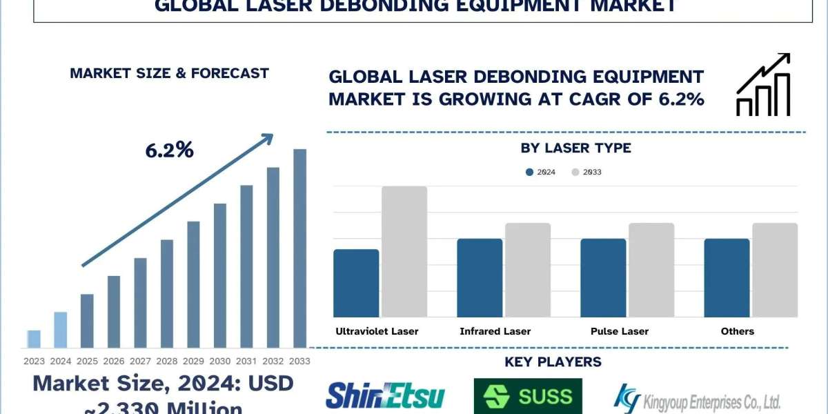
According to a new report by UnivDatos, The Laser Debonding Equipment Market is expected to reach USD million in 2033 by growing at a CAGR of 6.2% during the forecast period (2025-2033). Major growth drivers for the global Laser Debonding Equipment market include semiconductor packaging technology, trends toward smaller electronic devices, and higher automation in manufacturing processes. These key industries—electronics, medical devices, automotive, and aerospace—use laser debonding systems for microfabrication operations to separate bonded materials with precision without inflicting damage. Adoption of thin wafer processing, 3D integrated circuits, and flexible electronics has increased the demand for high-precision laser solutions. Laser systems integrated with smart manufacturing technologies, robotics, AI for quality control, and IoT-based monitoring have proven strong in improving the operational efficiency and scalability of manufacturing environments. The rise of advanced laser technologies like ultrafast lasers and AI-integrated systems is creating a paradigm shift in the industry's expectations regarding precision, speed, and reliability in the debonding process.
Access sample report (including graphs, charts, and figures): https://univdatos.com/reports/laser-debonding-equipment-market?popup=report-enquiry
In line with the rising demand for Laser Debonding Equipment, the following are some of the key updates:
- In 2024, Brewer Science Inc. presented its latest research development on the next-generation 3D packaging material with a thin-wafer processing technique. The hybrid bonding is used in advanced packaging and is cost-effective and reduces defectiveness in 3D printing.
- In 2024, Resonac Corporation developed a temporary bonding film and laser debonding process using xenon flashlight to debond wafers in the semiconductor manufacturing process.
Segments that transform the industry
- Based on Technology, the global laser debonding equipment market is segmented into Laser-Induced Breakdown Spectroscopy, Laser Ablation, and Laser-Induced Forward Transfer. Among these segments, laser ablation has held the largest share of the market due to factors like its precision, low material damage, and suitability for multiple applications. Laser ablation helps clean and non-contact removal of materials from a substrate, thereby making it appropriate for delicate semiconductor wafers and advanced packaging processes. The increasing demand for ultrathin wafers and the miniaturization of components in devices such as smartphones, wearables, and other electronics are further driving its adoption. Also, laser ablation systems offer increased manufacturing throughput and yield due to their faster processing and better compatibility with automation. Throughout the years, advances in ultrafast and femtosecond laser technology have also made laser ablation energy-friendly and cost-effective options for industries seeking a scalable, high-performance tool for reaching their debonding needs. Increasing adoption in the medical domain and flexible electronics further array activity in the market.
According to the report, the advancement in semiconductor packaging across the globe has been identified to be a key driver for market growth. Some of how this impact has been felt include:
Over the last few years, semiconductor packaging has witnessed significant changes, owing to the demand for next-generation electronic devices with high power levels, compact dimensions, and efficient designs. Yet, traditional packaging conventions are being replaced by radical approaches such as 3D Integrated Circuits (3D ICs), System-in-Package (SiP), and Fan-Out Wafer-Level Packaging (FOWLP). These advanced technologies offer high transistor density, better electrical performance, and good thermal management for next-generation devices such as smartphones, data centers, AI processors, and IoT components.
Laser debonding systems have been instrumental in the advanced packaging processes. Bonding substrates transiently is common during wafer handling and processing. Laser debonding represents the most precise method of debonding these structures without contacting and harming fragile structures. This becomes especially important in the context of thin-wafer applications, where any mechanical stress via conventional debonding methods could end up breaking the wafer and consequently lead to a loss of yield.
Click here to view the Report Description & TOC https://univdatos.com/reports/laser-debonding-equipment-market
Needless to say, as chip manufacturers shrink die dimensions and make their performance more demanding, the pressure on these debonding methods becomes stronger. These laser-based methods provide reliable, efficient, and damage-free debonding with the required precision and speed for successful integration into automated manufacturing systems. Laser debonding equipment is thus an integral enabling technology for the domain of semiconductor packaging technology going forward.
Related Report:-
Laser-Induced Breakdown Spectroscopy Market: Current Analysis and Forecast (2023-2030)
Welding Torch and Tip Changing Robotic Station Market: Current Analysis and Forecast (2024-2032)
Tunable Laser Market: Current Analysis and Forecast (2023-2030)
Industrial Automation Market: Current Analysis and Forecast (2024-2032)
MENA Manufacturing 3D Printing Market: Current Scenario and Forecast (2019-2025)
Contact Us:
UnivDatos
Contact Number - +1 978 733 0253
Email - [email protected]
Website - www.univdatos.com
Linkedin- https://www.linkedin.com/company/univ-datos-market-insight/mycompany/